
Having already understood the basic introduction of NADC24, if there are any unclear points, you can refer to the previous article on the introduction of NADC24.
Introduction to Nuvoton NuMicro 24-bit Analog-to-Digital Converter (ADC)
Start of the Article
The NADC24 uses the SPI (Serial Peripheral Interface) communication protocol, which is a widely used synchronous serial communication standard for data exchange with a host device. The SPI interface of the NADC24 includes the following four pins: SPI_SS, SPIDO, SPIDI, and SPI_CLK.
Operating Phases
- Initialization and Wake-up:
- After the first power-on or wake-up from power-down mode, the NADC24 requires 250 μs of stabilization time to ensure the internal circuits are fully initialized before starting ADC conversion.
- SPI Clock Rate and Duty Cycle:
- The maximum operating frequency of SPI_CLK is 20 MHz, meeting the requirements for high-speed data transmission.
- The duty cycle of the clock signal must be controlled within the range of 40% to 60% to avoid timing errors that could lead to unstable data transmission.
- SPI Data Transmission:
- Data is transmitted in 8-bit frames, with the first frame containing a command byte used to specify the operation mode, register settings, or data read instructions.
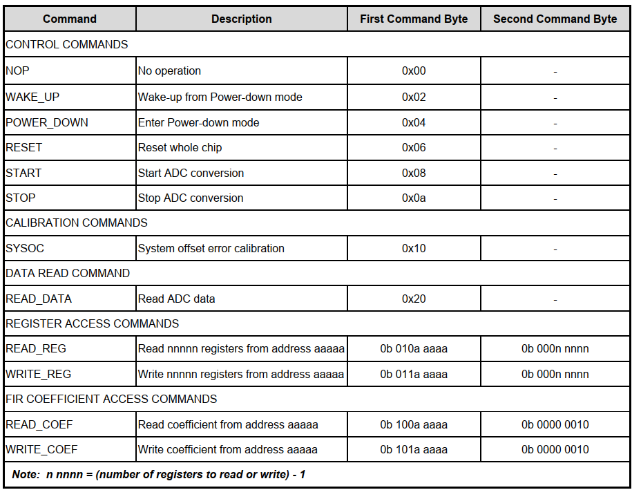
Command Table
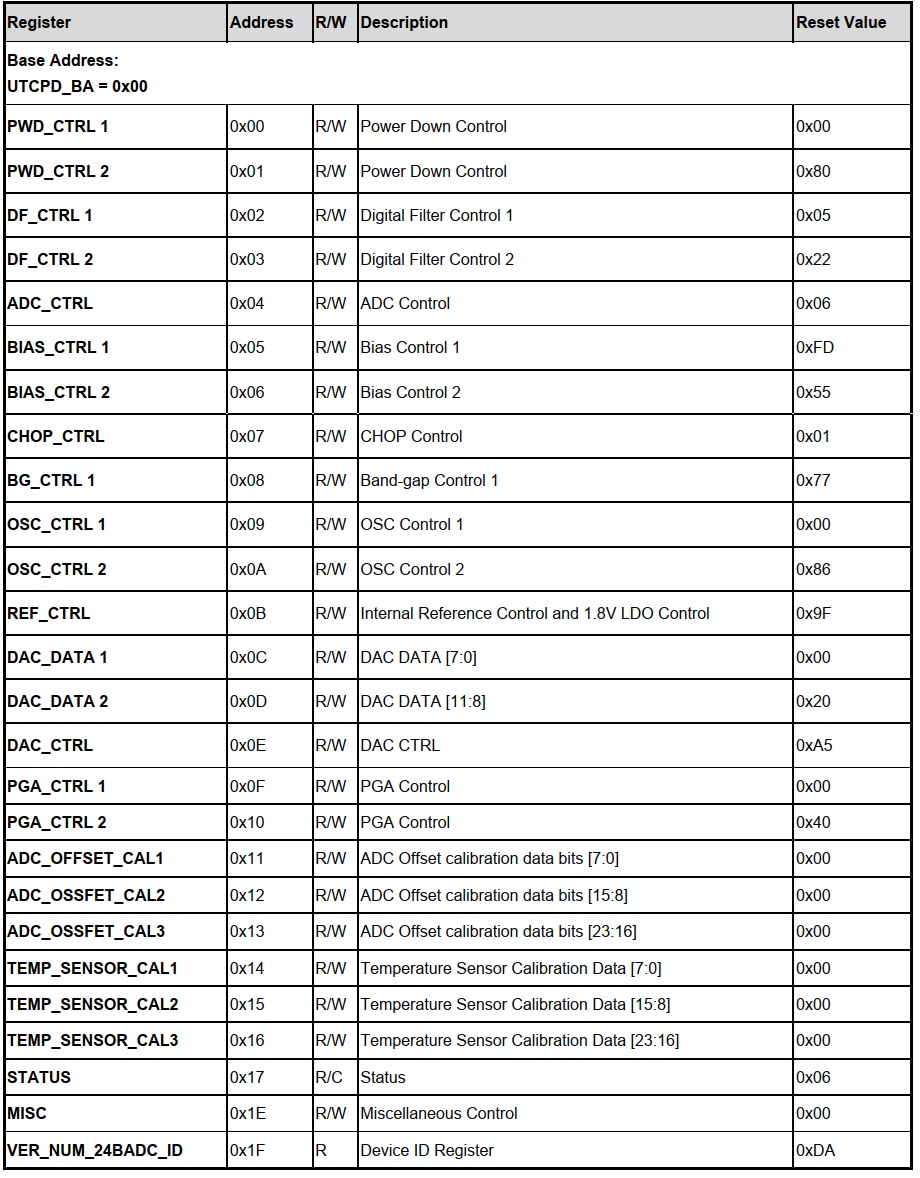
Register Map
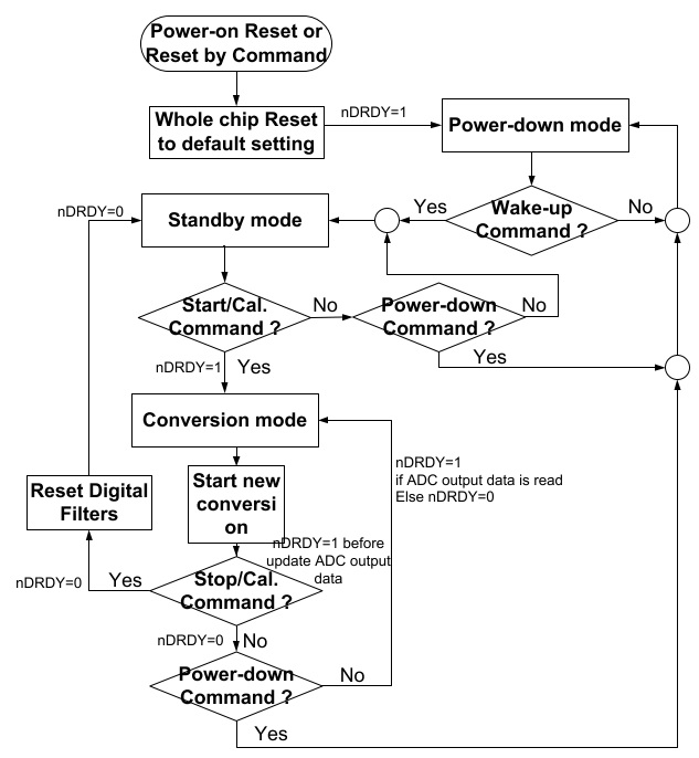
ADC Operating Flow Chart
1. Standby Mode
-
Default mode upon startup:
The device automatically enters standby mode after power-on. When no ADC conversion is in progress, the device also enters standby mode. -
Features and Advantages:
- In standby mode, the device is in an inactive state, significantly reducing power consumption.
- When starting a conversion from standby mode, no additional delay is required; the conversion begins immediately upon receiving the START command.
-
Entry Conditions:
- The device enters standby mode upon receiving the STOP command, waiting for new instructions.
2. Conversion Mode
-
Mode Activation:
Upon receiving the START command, the ADC enters conversion mode and continuously performs analog-to-digital conversion until the STOP command is received to halt the conversion. -
Limitations and Considerations:
- In conversion mode, the digital filter settings (DF_CTRL) cannot be changed to avoid interference with the ongoing conversion.
- This mode is designed to support long-term or continuous analog-to-digital conversion operations.
3. Power-Down Mode
-
Mode Activation:
Upon receiving the POWER_DOWN command, the device enters power-down mode. This mode is designed to achieve the lowest power consumption, suitable for applications requiring long idle periods. -
Features and Advantages:
- All analog and digital circuits are turned off to save power.
- Register Values Retained: In power-down mode, all register values remain unchanged, allowing for quick recovery to the working state upon wake-up.
-
Exit Conditions:
- The device exits power-down mode and enters standby mode only upon receiving the WAKE_UP command. It then waits for the START command to enter conversion mode.
Overview of Operating Modes and Switching Logic
-
Power-on Reset or Reset by Command
- When the device is powered on or a reset command is executed, the entire chip is reset to its default settings and enters standby mode.
-
Standby Mode
- In the default state, the device is in standby mode, ready to receive further instructions.
- Switching Conditions:
- If a START or Calibration Command is received, the device enters conversion mode.
- If a Power-down Command is received, the device enters power-down mode.
- If no further commands are received, the device remains in standby mode.
-
Conversion Mode
- In this mode, the ADC continuously performs analog-to-digital conversion until a stop or calibration command is received.
- Switching Conditions:
- Data Ready Flag (nDRDY): Indicates whether the data is ready:
- If the data is read,
nDRDY = 1; otherwise,nDRDY = 0.
- If the data is read,
- If a stop command is received, the device returns to standby mode.
- If a power-down command is received, the device enters power-down mode.
- Data Ready Flag (nDRDY): Indicates whether the data is ready:
-
Power-down Mode
- In this mode, all analog and digital circuits are turned off to achieve the lowest power consumption.
- Switching Conditions:
- Upon receiving a wake-up command, the device enters standby mode.
- If no wake-up command is received, the device remains in power-down mode.
Quick Initialization and Usage Flow of NADC24
Nuvoton provides a complete set of APIs for the NADC24, simplifying the developer's usage process. According to the official reference example, the complete initialization and conversion operation can be completed with the following three lines of commands:
1. Reset and Initialization
/* Init NADC24 */
Reset_NADC24(); // Reset NADC24
NADC24_Cali_and_Initial(CALI_NADC24); // Perform calibration
NADC24_Cali_and_Initial(INIT_NADC24); // Complete initialization
- Purpose:
By configuringREG_ADDR_PWD_CTRL1, disable the internal DAC module and its buffer to save unnecessary power consumption. - Register Settings:
PWD_CTRL1_PWD_DAC_Msk: Controls the DAC module power.PWD_CTRL1_PWD_DACBUF_Msk: Controls the DAC buffer power.
Purpose:
Disable unused buffer modules to reduce power consumption.
- Purpose:
Use the internal oscillator to avoid the need for an external clock. - Frequency Selection:
Configure to49.152 MHzto meet precise timing requirements.
Purpose:
Provide a stable internal reference voltage for the ADC, avoiding the use of an external voltage reference.
Differences between Calibration Mode and Initialization Mode:
- Calibration Mode: Disable the FIR filter (
DF1_CTRL_BYPASS_FIR_DISABLE). - Initialization Mode: Enable the FIR filter (
DF1_CTRL_BYPASS_FIR_ENABLE).
Clock Frequency: Set to
1.024 MHz to meet the internal modulator requirements.Adjust the PGA bias current, affecting gain and response speed.
Gain Configuration:
PGA gain settings are selected based on usage scenarios.
- Disable offset correction, suitable for calibration mode.
2. Start Analog-to-Digital Conversion
- Enter Conversion Mode:
Send the START command to initiate analog-to-digital conversion. - Data Reading:
Read the conversion results via the SPI interface (refer to the SPI command format and timing diagram).
3. Stop Conversion or Enter Standby Mode
- Stop Conversion:
Send the STOP command to end the current conversion and enter standby mode. - Enter Power-Down Mode:
Send the POWER_DOWN command to reduce power consumption and switch to power-down mode.
4. Repeat Operations
Based on application requirements, developers can repeatedly perform the following operations:
- Start analog-to-digital conversion.
- Read data.
- Stop conversion or switch modes.
This process ensures system flexibility and efficiency, suitable for various high-precision measurement needs.
Conclusion and Recommendations
AdjustabilityThe code implements comprehensive configuration and calibration through APIs, allowing developers to flexibly modify relevant parameters based on application needs, adapting to diverse application scenarios.
Application Scenarios
The NADC24 is suitable for high-precision measurement applications (e.g., high-precision sensors), fully leveraging its performance advantages to meet precision measurement requirements.