
For many people involved in PCB layout design, RF routing often involves issues such as analog signals, EMC (electromagnetic compatibility), and impedance matching. As a result, designers typically refer to the recommendations provided in chip manuals during the design process. For instance, when RF routing requires compatibility design, it is common to use a method where two overlapping packages share the routing. The purpose of this approach is to prevent signal radiation at corners caused by discontinuities in RF signal impedance.
This article uses real-world examples to share how to address co-layout (co-placement) issues for RF modules in PCB design.
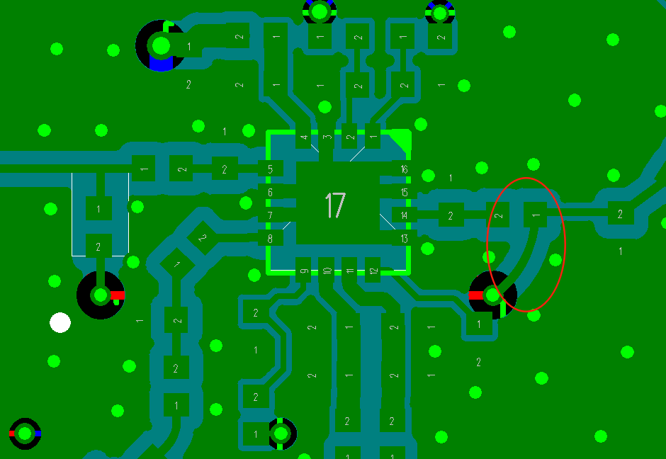
As shown in the figure below, this is the layout design of the FEM RF module in Client A's product. A branching point is designed at both ends of the FEM module, primarily for compatibility purposes. However, the key issue is that the components are not truly co-laid out; their orientation is merely adjusted through RF lines. This approach effectively adds an extra segment of wire to the RF path, resulting in characteristic impedance mismatch for the entire section, which in turn causes EMI problems.
As shown in the figure below, we measured the current characteristic impedance status using a network analyzer and found it to be in a mismatched state. Effective improvement can no longer be achieved through component matching adjustments.

The adjustment strategy for this situation is to add an extra 0-ohm resistor in the common layout. In RF circuits, a common layout approach is often used, where shared footprints are utilized to achieve path overlap and avoid EMI interference caused by impedance mismatch. As shown in the figure below, by overlapping the pads of two components with the same footprint, not only can the residual segments of 90-degree turns be reduced, but impedance continuity can also be ensured.

1. What is RF Co-layout?
RF Co-layout refers to the process of reasonably arranging multiple RF components or system elements in physical space during design and manufacturing to minimize interconnections between them while maximizing the efficiency and reliability of signal transmission.
2. Why is RF Co-layout so important?
RF Co-layout can reduce signal interference, improve system performance, lower power consumption, optimize space utilization, and reduce manufacturing costs.
3. What are the main challenges of RF Co-layout?
Challenges include electromagnetic interference (EMI) between components, thermal effect management, signal integrity, and the complexity of interconnections.
4. How to evaluate the effectiveness of RF Co-layout?
Evaluation can be conducted through signal integrity analysis, electromagnetic compatibility testing (EMC), and actual performance testing.
5. How does RF Co-layout affect system power consumption?
A reasonable layout can reduce unnecessary signal transmission losses, thereby lowering system power consumption.